


Design , consulting Prototyping ; PCB technology , specialize IC Test Load board
- 38 people Following this
- 101 Posts
- 32 Photos
- 80 Videos
- 0 Reviews
- Science and Technology
- ADiTECH
- 0816258882 & what app
- Bangbuathong, Nonthaburi
Recent Updates
- KiCad PCB design for all in one
- Schematic
- PCB design with 3D
Note : a lot library for schematic , PCB and 3D components
- Gerber
- Utility functions
- PCB copy
Note:
Download : https://www.kicad.org/download/
Sample training : https://www.youtube.com/watch?v=3FGNw28xBr0KiCad PCB design for all in one - Schematic - PCB design with 3D Note : a lot library for schematic , PCB and 3D components - Gerber - Utility functions - PCB copy Note: Download : https://www.kicad.org/download/ Sample training : https://www.youtube.com/watch?v=3FGNw28xBr00 Comments 0 Shares 250 Views 0 Reviews1
- EP 51 Make PCB แบบ DIY by using 3D resin printer
ทำ PCB จาก 3D resin printer แบบเต็มรูปแบบ Fix bug มี 2 แบบให้เลือก ทั้ง Positive & Negative PCB dry film
3D Resin printer มีลำแสง UV 405 nM เหมาะสำหรับ PCB dryfilm
Software ที่ใช้
gerbv ใช้แปลงไฟล์ Gerber เป้น SVG
Inkscape ใช้เปิด SVG และ save file เปลี่ยน Raster เป็น vector file.
CAM350 change positive gerber to Negative gerber
Bambu Studio ใช้ Import SVG file to 3D file ( STL and etc.. ) and export
Use STL program to 3D resin printer make PCB DIY
Note : วิธีต่างจากของฝร้่งEP 51 Make PCB แบบ DIY by using 3D resin printer ทำ PCB จาก 3D resin printer แบบเต็มรูปแบบ Fix bug มี 2 แบบให้เลือก ทั้ง Positive & Negative PCB dry film 3D Resin printer มีลำแสง UV 405 nM เหมาะสำหรับ PCB dryfilm Software ที่ใช้ gerbv ใช้แปลงไฟล์ Gerber เป้น SVG Inkscape ใช้เปิด SVG และ save file เปลี่ยน Raster เป็น vector file. CAM350 change positive gerber to Negative gerber Bambu Studio ใช้ Import SVG file to 3D file ( STL and etc.. ) and export Use STL program to 3D resin printer make PCB DIY Note : วิธีต่างจากของฝร้่ง 0 Comments 0 Shares 479 Views 0 Reviews
 - วิธีทำpcb จาก 3D resin printer จะเป็นแบบ DLP หรือ SLA ก็ได้
https://youtu.be/-Qeq7ZgUOuE?si=peawebjWDgbXmkYTวิธีทำpcb จาก 3D resin printer จะเป็นแบบ DLP หรือ SLA ก็ได้ https://youtu.be/-Qeq7ZgUOuE?si=peawebjWDgbXmkYT0 Comments 0 Shares 353 Views 0 Reviews - More VDO Sprint in English version
https://youtu.be/g0nkLJ4YQ2c?si=ndmnfKI3GQ64iR-pMore VDO Sprint in English version https://youtu.be/g0nkLJ4YQ2c?si=ndmnfKI3GQ64iR-p0 Comments 0 Shares 255 Views 0 Reviews - DC to AC converter
ผมมีรุ่น 1000 Watts อยู่ในมือและทำ PCB ขึ้นมาใหม่และปรับปรุงให้ดีถาม link นี้ มีความคืบหน้าจะนำมาเสนอต่อไป
ตัวผมเองติด Solar cell จะลองทำ On Grid กลางคืน
์Note : ตัวอย่างใน youtube หน้าจะ 500 Watts
Link https://www.youtube.com/watch?v=jISNRNdQKU8
DC to AC converter ผมมีรุ่น 1000 Watts อยู่ในมือและทำ PCB ขึ้นมาใหม่และปรับปรุงให้ดีถาม link นี้ มีความคืบหน้าจะนำมาเสนอต่อไป ตัวผมเองติด Solar cell จะลองทำ On Grid กลางคืน ์Note : ตัวอย่างใน youtube หน้าจะ 500 Watts Link https://www.youtube.com/watch?v=jISNRNdQKU8 0 Comments 0 Shares 340 Views 0 Reviews
 - ตัวอย่างการลอกแบบจาก Sprint 6(Good sample from Sprint 6)
https://www.youtube.com/watch?v=dOc2LUxs4Xw&t=11sตัวอย่างการลอกแบบจาก Sprint 6(Good sample from Sprint 6) https://www.youtube.com/watch?v=dOc2LUxs4Xw&t=11s0 Comments 0 Shares 238 Views 0 Reviews - อีกทางเลือกในการ copy PCB คงเป็น clip สุดท้ายของเรื่องการ copy PCB ทุกคนคงได้แนวทางกันไปจนครบ.
วิธีอื่นผมไม่มีเครื่องมือ จะทำอธิบายอยาก เช่น x-ray scan ( ทำได้มากกว่า 2 เลเยอร์ ) อีกวิธี คือ
scan & re-digitizer ( ต้องมี flying probe )
วิธีของผมคงทำได้ 1-2 เลเยอร์ อาจทำได้ถึง 4 เลเยอร์ แต่ก็อยากอีกทางเลือกในการ copy PCB คงเป็น clip สุดท้ายของเรื่องการ copy PCB ทุกคนคงได้แนวทางกันไปจนครบ. วิธีอื่นผมไม่มีเครื่องมือ จะทำอธิบายอยาก เช่น x-ray scan ( ทำได้มากกว่า 2 เลเยอร์ ) อีกวิธี คือ scan & re-digitizer ( ต้องมี flying probe ) วิธีของผมคงทำได้ 1-2 เลเยอร์ อาจทำได้ถึง 4 เลเยอร์ แต่ก็อยาก0 Comments 0 Shares 313 Views 40 0 Reviews - Down load Sprint Layout ได้ที่นี้ฟรี
https://forum.arduino.cc/t/free-pcb-software/1168493Down load Sprint Layout ได้ที่นี้ฟรี https://forum.arduino.cc/t/free-pcb-software/1168493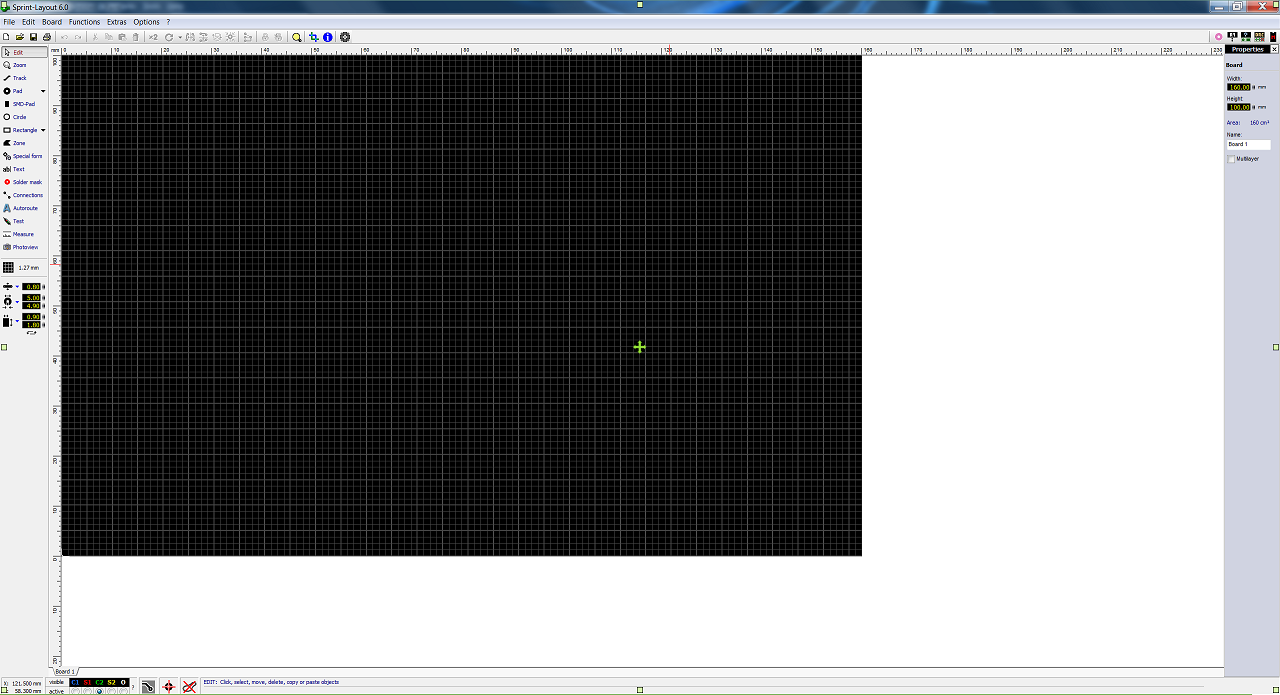 0 Comments 0 Shares 304 Views 0 Reviews
 - แนะนำ และ ชอบ Project DIY UNIVERSAL Step up & Down DC to DC converter
สามารถนำไปใช้ได้หลายหลากหลาย เช่น ใช้ร่วมกับ Solar Cell ชาร์จ Battery หรือเป็นแหล่งจ่ายไฟ
วงจรไม่ยาก อธิบายละเอียด มีการทดสอบวงจรให้ดู
ผมอาจออกแบบแผงวงจรให้ คน Down load gerber ไปใช้
https://www.youtube.com/watch?app=desktop&v=9wsVshsJ11oแนะนำ และ ชอบ Project DIY UNIVERSAL Step up & Down DC to DC converter สามารถนำไปใช้ได้หลายหลากหลาย เช่น ใช้ร่วมกับ Solar Cell ชาร์จ Battery หรือเป็นแหล่งจ่ายไฟ วงจรไม่ยาก อธิบายละเอียด มีการทดสอบวงจรให้ดู ผมอาจออกแบบแผงวงจรให้ คน Down load gerber ไปใช้ https://www.youtube.com/watch?app=desktop&v=9wsVshsJ11o0 Comments 0 Shares 392 Views 0 Reviews - ขออนุญาติผลงานออกแบบและทำบอร์ดต้้นแบบประเภท High Layer Counter บอร์ดประเภทนี้ลูกค้าจะสั่งทำประมาณ 1-3 Boards เท่านั้น
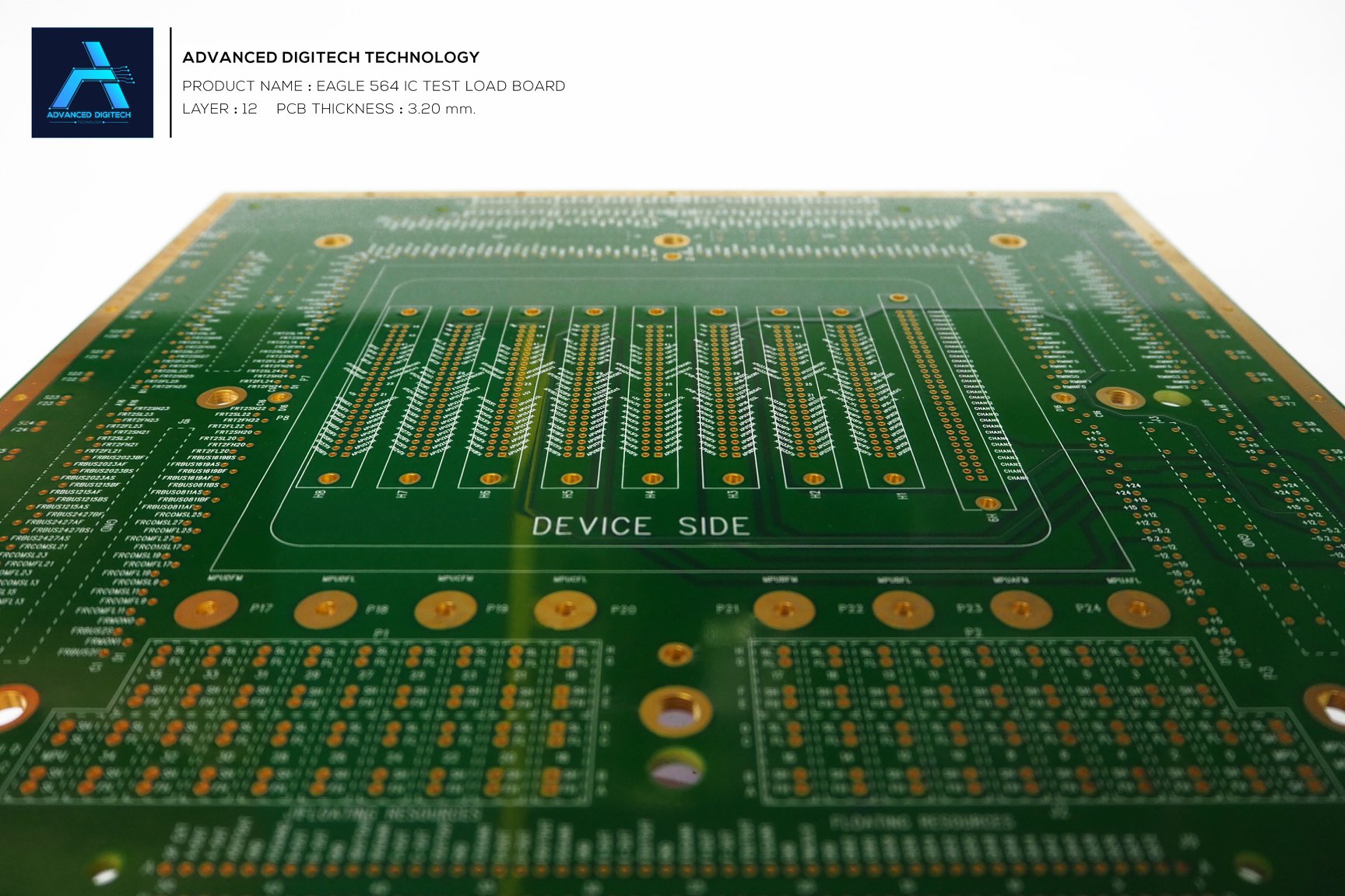
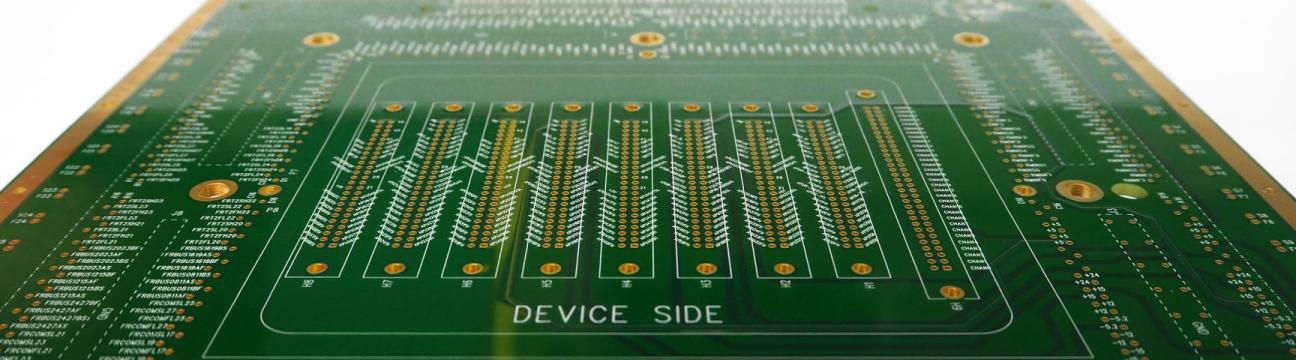
ทางขาวมือเป็น 12 Layers หนา 5.80 mm
ทางซ้ายมือเป็น 26 Layers หนา 5.80 mm
เคลือบผิวด้วยทองหนา 35 micro inch
เราเรียก Boards เหล่านี้ว่า IC Test Load Board มันใช้ทดสอบ IC ตามมาตรฐานโรงงานผลิต IC
ทั้งสองบอร์ดทำจากประเทศไต้หวั่น ไม่ได้ทำจากประเทศจีน
ขออนุญาติผลงานออกแบบและทำบอร์ดต้้นแบบประเภท High Layer Counter บอร์ดประเภทนี้ลูกค้าจะสั่งทำประมาณ 1-3 Boards เท่านั้น ทางขาวมือเป็น 12 Layers หนา 5.80 mm ทางซ้ายมือเป็น 26 Layers หนา 5.80 mm เคลือบผิวด้วยทองหนา 35 micro inch เราเรียก Boards เหล่านี้ว่า IC Test Load Board มันใช้ทดสอบ IC ตามมาตรฐานโรงงานผลิต IC ทั้งสองบอร์ดทำจากประเทศไต้หวั่น ไม่ได้ทำจากประเทศจีน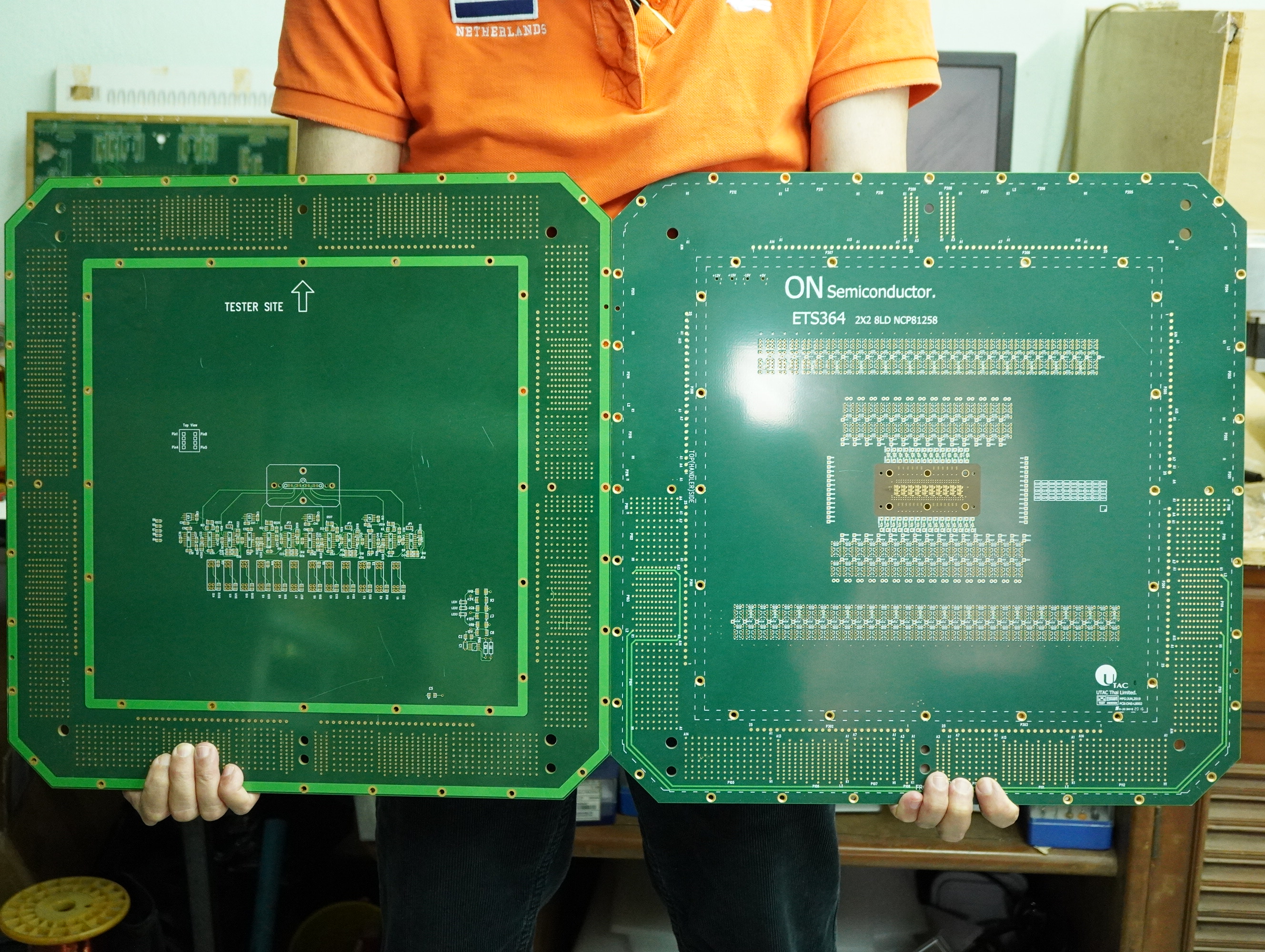 0 Comments 0 Shares 337 Views 0 Reviews
 - มาดูของฝรั่งเขาสอนตัวเดียวกับผมบาง ตาม link นี้ครับ
https://www.youtube.com/watch?v=Kk3b--5zkc8&list=PLzVsLVsxIwiYAKuaFiAfB-UTd3hS_3a21มาดูของฝรั่งเขาสอนตัวเดียวกับผมบาง ตาม link นี้ครับ https://www.youtube.com/watch?v=Kk3b--5zkc8&list=PLzVsLVsxIwiYAKuaFiAfB-UTd3hS_3a210 Comments 0 Shares 293 Views 0 Reviews
More Stories